[ad_1]
In context: As we strategy the 2nm course of node, some roadblocks are rising that might additional stagnate the already gradual Moore’s Regulation progress. One problem is the right way to effectively distribute energy to tens of billions of tiny transistors utilizing copper wiring with out eroding efficiency features. Now, Utilized Supplies, a significant provider of semiconductor manufacturing gear, believes it has the reply.
Final week, Utilized Supplies pulled again the curtain on its newest supplies engineering options designed to allow copper wiring to scale all the way down to 2nm dimensions and under whereas additionally decreasing electrical resistance and strengthening chips for 3D stacking.
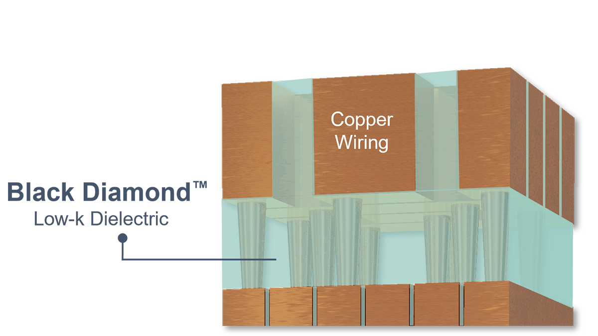
The corporate’s Black Diamond low-k dielectric materials has been provided because the early 2000s. It surrounds copper wires with a particular movie engineered to scale back the buildup {of electrical} prices that enhance energy consumption and trigger interference between electrical indicators.
Utilized Supplies has now come up with an enhanced model of Black Diamond, which reduces the minimal k-value even additional, enabling copper wiring scaling to the 2nm node whereas additionally rising mechanical energy – a essential property as chipmakers look to stack a number of logic and reminiscence dies vertically.
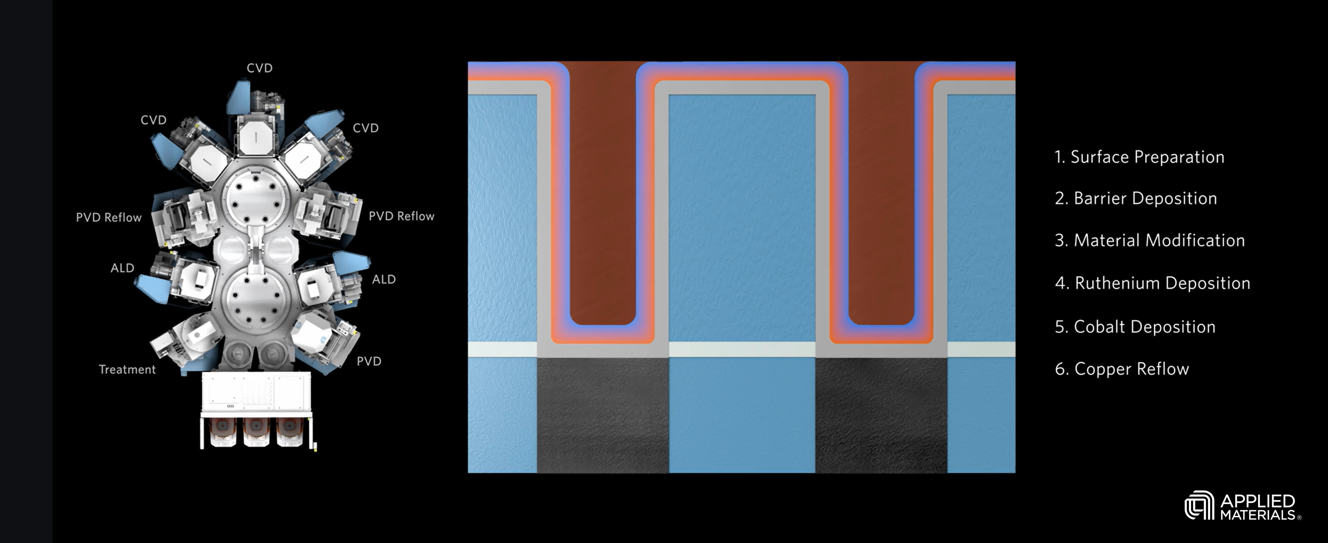
However scaling the copper wiring itself as dimensions shrink is one other huge problem. At this time’s most cutting-edge logic chips can pack over 60 miles of copper wires which might be customary by first etching trenches into the dielectric materials after which depositing an ultra-thin barrier layer to forestall copper migration. A liner layer goes down subsequent to assist copper adhesion earlier than the ultimate copper deposition fills the remaining house.
The issue is that at 2nm dimensions and under, the barrier and liner layers eat an more and more massive share of the out there trench quantity, leaving little room for adequate copper fill and risking excessive resistance and reliability points. Utilized Supplies has solved this predicament with this brand-new supplies concoction.
Their newest Built-in Supplies Resolution (IMS) combines six totally different core applied sciences into one high-vacuum system, together with an industry-first pairing of ruthenium and cobalt to type an ultra-thin 2nm binary metallic liner. This permits a 33% discount in liner thickness in comparison with earlier generations whereas additionally bettering floor properties for seamless, void-free copper adhesion and reflow. The top result’s as much as 25% decrease electrical resistance in chip wiring to spice up efficiency and scale back energy leakage.
Utilized Supplies claims that every one main logic chipmakers have already adopted its new copper barrier seed IMS with ruthenium CVD know-how for 3nm chip manufacturing, with 2nm nodes anticipated to observe.
The corporate additionally estimates its complete served out there marketplace for chip wiring options will swell from round $6 billion per 100,000 wafers beginning at present to over $7 billion with the introduction of bottom energy supply schemes.
[ad_2]